As you might have read I recently started to document the assembly of Benjamin Vedders insane 12S 50A (240A peak) motor controller called VESC. This is the third post in this series. In the previous VESC article I showed you how to cut a stencil for solder paste application on your own. This time I am going to show you how to use the stencil to populate a VESC 4.12 PCB with all the tiny components.
In order to make the alignment process easier I designed a small holder for the pcb. You can print this file on a 3D printer and insert the PCB into this holder. Take some adhesive tape and fixate the PCB from the back. Add and align the stencil before using more adhesive to fixate the stencil to the holder as well. Apply some solderpaste and use a plastic scraper (credit card) to spread the solder paste on the stencil like this:
You can now carefully remove the adhesives, stencil, and the holder while trying sure not to smear the solder paste all over the PCB 😉 When you succeed it should look like the following picture. If the first try does not look clean enough, use some isopropyl alcohol and clean the board and stencil before repeating the paste application.


Do not worry to much about the perfect placement. Most of the tiny parts will be dragged in place by the surface tension of the solder paste during the reflow process. Just make sure the bigger and heavy parts such as the mosfets are perfectly aligned to the pads. Now it is time to reflow the board. The recommended way of “baking” this kind of PCB is to use a reflow- or modified pizza oven. You can also use a hot air station for this purpose. Make sure to pre-heat the whole board with circling motions before soldering the single items. Ah and before you melt your workspace mat as well — I heard it might be a good idea to use a heat resistant surface below the PCB during heat application 😉
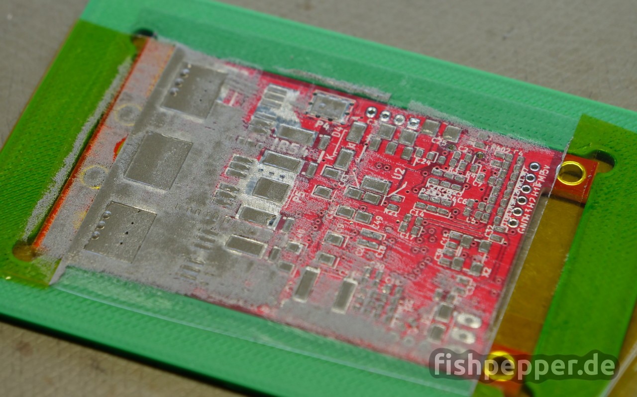
Once you finished the soldering, make sure to let the board cool down properly. Your PCB will now (hopefully) look similar to this:

Now comes the boring part, rinse and repeat…
Flip the board over and apply solder paste again. This time I messed it up a bit, you can see some offset in the paste alignment. Do not worry to much about it, this offset is still fine to work with.

Now place the parts as done before, make sure to align the fine pitched STM32 and mosfet driver properly.

The board will now be reflow soldered the second time. Do not worry about the parts you have already mounted on the back. The parts will stick to the board as the temperature is usually a bit lower and the surface tension helps to keep the parts in place. Do not be shocked when the soldering is done, most likely you will have some shorts at the STM32, the mosfet driver IC, and the USB port as well.

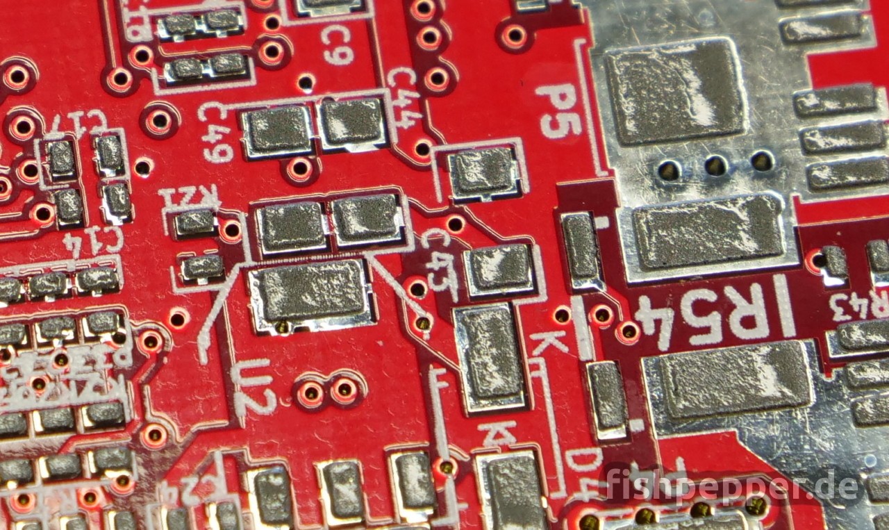
Take some solder wick, good flux, and some time to carefully remove the solder bridges. I prefer doing this under the cheap stereo microscope which I recently bought for this purpose. Take your time to check all parts for shorts and not properly soldered pads. The mosfet driver IC has some pads connected to each other. This makes it hard to remove solder bridges at those spots. Double check the PCB layout where the bridged pads are, you can leave the solder bridges in place there. When done, your board should look like this:

That’s all for today. Further updates on my progress of the VESC assembly and setup will follow soon.
You can find the previous VESC articles here:
- Tutorial: Initial flashing a new born VESC (10/31/2017)
- Tutorial: VESC assembly — A tale of PCBs, stencils, solderpaste, and damned hot air (9/24/2017)
- VESC / DIY: How to cut SMD solderpaste stencils yourself using a Silhouette craft plotter (9/17/2017)
- 3S, 4S, 5S, 6S ?? — nah… Let’s go 12S/50A (240A Peak)! (9/12/2017)