I recently started to assemble a VESC brushless motor controller on my own. This is the second post in this series. As you all might know I do a lot of prototyping. Nowadays you can get your custom PCBs made at a very low price. I get most of my prototypes done at OSHPark.com. Three copies of your design come at $5 per square inch and shipping is free. The bad part (at least for me) is that OSHPark is located in the US, it usually takes two more weeks for shipping to germany. When I am in a rush I order my prototypes at multi-circuit-boards (39€ for 10x10cm). PCB Assembly can be speed up by an enormous amount of time by using a solderpaste stencil. Up to now I have used different services for that. Most of the time they are either slow or comparable expensive. This is why I started to cut the smd paste stencils on my own.
The Cutter
 As it turned out you can cut yourself a stencil on the cheap by using an electronic craft cutting tool. I bought the cheap Silhouette Portrait for this task. This cutter connects to your PC using an USB port and uses a small blade to cut paper, cardstock, vinyl, fabric and more, up to 8 inches wide and 10 feet long. I have sucessfully used it in the past to cut iron-on foil to decorate t-shirts and other fabric. Most commercial paste stencils are made out of thin laser cut steel- or kapton sheets. As we are not going to use a laser to cut the material, we can use a cheaper plastic that would otherwise melt or burn. I use one half of Fellowes Impress 100 laminating pouches. Some others used transparency films as the stencil material in the past. Most of the available transparency films will do, some cut better and some worse. Just make sure to get them in a thickness of around 100 micron (0.1mm).
The normal silhouette cutting blades that are embedded in a plastic holder are quite pricey, I prefer to use normal cutting blades available everywhere. In order to use these cheap standard cutting blades a matching adapter or holder is needed. I bought this CB09 adapter that comes with a set of ten 60° blades for a fraction ($8) of the cost of a single original blade. The 60 degree blades are the best for cutting such small details as we will do.
Preparations
Y ou will need to export a stencil mask gerber file from within your CAD software. I am going to show you the process of exporting in Kicad. If you use a different EDA software the steps will be similar.
Start by opening your finished board design. Click on Dimensions -> Part Masks Clearance and modify the “Solder paste ratio clearance” to -10%. This will make the solder paste pads slightly smaller than the copper pads. If you experience a lot of solder bridges you can try -15%. But usually -10% is a good starting point. Now it is time to export the gerber files. Click on File -> Plot and select the Paste layers (F.Paste and B.Paste) and click “plot”.
We are going to use a special toolchain optimized for cutting stencil masks. The program that comes with the Silhouette Portrait does a good job for craft cutting but it is not very good at cutting the tiny pads we need for our stencils. Peter Monta did a really great job by creating the gerber2gpraphtec toolchain. His collection of tools analyzes the gerber file and sends specific, optimized motion commands to the plotter. His approach tries to cut drawn line segments separately, uses anti backlash techniques, and features drag-knife-angle “training”. Start by cloning his git repository:
git clone https://github.com/pmonta/gerber2graphtec.git
cd gerber2graphtec
There is a good amount on how to install the dependencies and a basic setup guide available in his README file. Make sure to have a look at it before proceeding. One big advantage of his toolchain is that you do not have to mess around with converting the output to any intermediate file formats, his tools will read the plain gerber output of your CAD software!
Cutting
The hardest part is finding the right cut depth for your stencil. For the normal blade a depth setting of “2” will most likely do its job. The before mentioned universal cutter needs some try and error cutting to find the right depth.
Take the adhesive backed cutting mat of your plotter and stick one of the transparency films to it. Hold it in front of the wheens and use the mat button to load it into the printer. When you run Linux you are now set, use the gerber2graphtec file to cut the stencil mask:
gerber2graphtec BLDC_4-F.Paste.gbr >/dev/usb/lp0
The cutting will now begin. Due to the way this script cuts the stencil the whole process will take a lot longer compared to the way the standard software does its job. Do not worry, just be patient. Here is a short demonstration of the cutting process:
In case you use a windows or mac machine I would recommend to browse and read this thread on dangerousprototypes. There are some hints and reports on using gerber2graphtec on non linux machines. I have no experience with that.
When the printer is done unload the foil and remove your stencil. Use a thin plastic card (e.g. credit card) do scrape of the tiny plastic parts that stick to your cutting mat. The finished stencil should look similar to this:


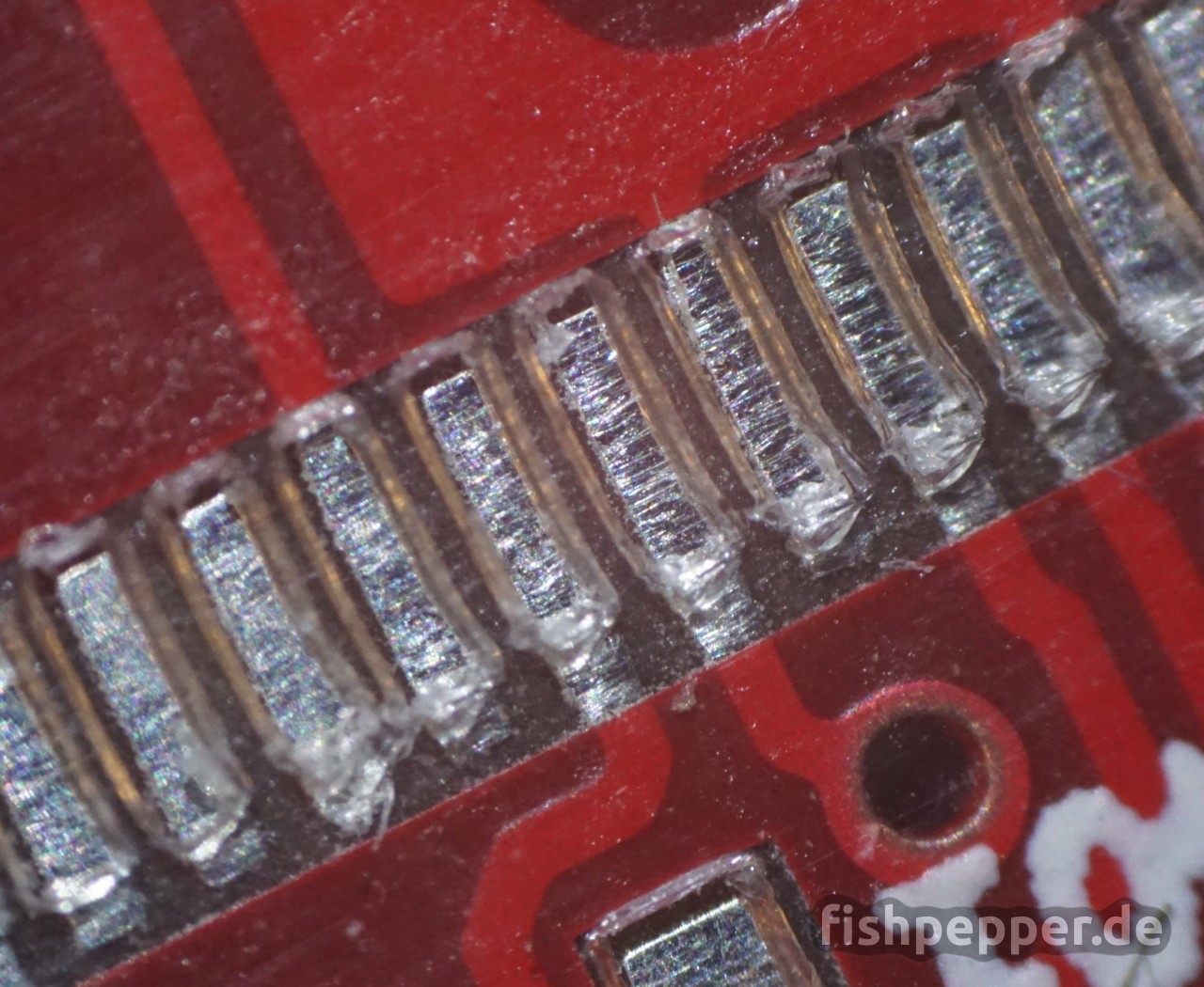
Even though the corners look a bit messy, this is perfectly fine. One would certainly want to have a clean and nice cut stainless steel stencil for mass manufacturing, for a one shot prototype this is more than fine. I have a final shot on how the solder paste application turned out:
That’s it for now. Further updates on my progress of the VESC assembly will follow soon.
- Tutorial: Initial flashing a new born VESC (10/31/2017)
- Tutorial: VESC assembly — A tale of PCBs, stencils, solderpaste, and damned hot air (9/24/2017)
- VESC / DIY: How to cut SMD solderpaste stencils yourself using a Silhouette craft plotter (9/17/2017)
- 3S, 4S, 5S, 6S ?? — nah… Let’s go 12S/50A (240A Peak)! (9/12/2017)